What is a 2 layer PCB?
Home < 2 layer pcb < What is a 2 layer PCB?
2024-03-14 09:42:36 2 layer pcb 13 Viewed
SummaryWhat is a 2 layer PCB?2-layer PCB (double-layer printed circuit board) is a design technology for electronic components whose main feature is the use of two layers of conductive material for wiring. The main advantage of this design is that it can reduce interference and electromagnetic interference...
What is a 2 layer PCB?
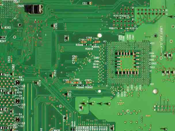
2-layer PCB (double-layer printed circuit board) is a design technology for electronic components whose main feature is the use of two layers of conductive material for wiring. The main advantage of this design is that it can reduce interference and electromagnetic interference (EMI) during signal transmission. In many cases, 2 layer PCBS are used to create smaller, lighter, and more reliable electronic devices.
How thick should a 2 layer PCB be?
The thickness of a 2-layer PCB usually depends on the specific application and design needs, the common 2-layer PCB thickness is 1.6mm, which is because 1.6mm is a universally available and affordable standard thickness, suitable for many applications.
2 Layer PCB Price
The 2 layer PCB price is affected by several factors:
1. Material cost: The type and quality of materials used in PCB manufacturing will directly affect the price. For example, high frequency or high-speed digital signals require special materials, which tend to be more expensive.
2. PCB size and shape: PCB size and shape will also have an impact on the price.
3. The number of layers and complexity: compared with multi-layer PCB, the number of layers is less, and the manufacturing and assembly process is relatively simple, so the price is relatively low; however, if the 2-layer PCB has a complex layout, high-density parts or special requirements, these factors may increase the manufacturing cost.
4. Quantity: Generally speaking, mass production will be more favorable than small batch or sample manufacturing.
5. Processing technology: Special process requirements (such as gold fingers, gold plating, etc.) will increase manufacturing costs.
6. Delivery time: If you need fast delivery, expedited production may add additional costs.
2 Layer VS 4 Layer PCB Difference
There are some differences between 2-layer PCB and 4-layer PCB in structure and function:
1. Structure: A 2-layer PCB is composed of two layers of copper foil and a medium layer, while a 4-layer PCB is composed of four layers of copper foil and three medium layers. 4-layer PCBS have more signal and power layers than 2-layer PCBS, which can provide better signal integrity and EMI/EMC performance.
2. Line layout: In a 4-layer PCB, the internal signal and power layer can be used for more complex wiring, helping to reduce signal interference, cross-coupling, and noise problems.
3. Signal integrity: Because there are more signal and power layers, 4-layer PCB can better control signal transmission and impedance matching, helping to improve signal integrity and anti-interference ability.
4. Heat dissipation performance: 4-layer PCB can be used for heat dissipation and thermal management due to an internal layer.
5 Complexity and cost: The design and manufacture of 4-layer PCBS is more complex than that of 2-layer PCBS, so the cost is usually higher. At the same time, designing a 4-layer PCB also requires more layout and wiring skills.
2 layer PCB stackup thickness
2 layer PCB stackup thickness refers to the overall thickness of the PCB board, usually determined by the thickness of the substrate and copper foil, the following are some common 2-layer PCB stack thickness ranges:
1. Substrate thickness: Common substrate thickness includes 1.6mm, 1.2mm, 1.0mm, etc., and other thickness can be selected according to demand.
2.Copper foil thickness: Common copper foil thicknesses include 1oz (about 35um) and 2oz (about 70um), and other thicknesses can be selected according to demand.
2 layer PCB design rules
In printed circuit board design, 2-layer PCB design rules usually refer to the design specification of dual panels, which includes wiring, power/ground wire distribution, component layout and other aspects of the content, as described below:
1. Wiring rules: the signal line should avoid crossing a large area of power supply/ground plane as far as possible to reduce interference and noise.
2. Power supply/ground wire design: the wiring between the power layer and the ground layer should be as close and evenly distributed as possible, so as to form a loop, reduce impedance and suppress noise.
3. Component layout rules: components with strong correlation should be as close to the layout as possible to reduce the signal transmission distance and improve system stability.
4. Other design rules: Considering the heat dissipation needs, high heat dissipation components should not be concentrated, and there should be sufficient heat dissipation path; keeping the symmetry of the design as much as possible helps to reduce signal transmission delay and electromagnetic interference.
2 layer PCB ground plane functions
1. Signal integrity: The ground provides a stable reference plane, which can effectively reduce the interference between the signal line and other layers.
2. Suppression of interference: The ground can absorb and disperse electromagnetic radiation and provide a low-impedance path, thereby reducing electromagnetic interference (EMI) and electromagnetic compatibility (EMC) problems.
3. Heat dissipation: The ground can be used as a heat dissipation path to help heat conduction and reduce the operating temperature of circuit components. Especially for components with large power consumption or applications requiring high reliability, a good heat dissipation design is necessary.
4. Ensure ground potential: The ground can provide a stable ground potential, ensure the common reference point between various circuit modules and components, and avoid the instability of the ground circuit or the generation of floating ground potential.
2 layer vs 4 layer PCB cost
2 layer vs 4 layer PCB cost can be affected by a number of factors including, but not limited to:
1. The number of layers: The manufacturing cost of a 4-layer PCB is usually higher than that of a 2-layer PCB because there are more layers and processing steps involved.
2. Plate type: Different types of plates have different costs, such as FR-4, high-frequency materials, etc.
3. Board thickness: The choice of board thickness will also affect the cost, usually thicker PCB will cost more.
4. Size: Large-size PCBS will usually cost more than small-size PCBS because more materials are required.
5. Design complexity: PCB with high design complexity, such as high-density wiring, special process requirements, etc., usually increases manufacturing costs.
6. Order quantity: Large orders can usually get a lower price, while small orders may cost more.
7. Special requirements: If there are special requirements, such as high impedance control, special surface treatment, blind holes/buried holes, etc., it may increase the manufacturing cost.
8. Manufacturing region: Manufacturing costs will also vary in different regions. For example, in some regions, labor costs are lower and may provide more competitive prices.
Previous:没有了!
Next:没有了!
2 layer pcb Description
What is a 2 layer PCB? Related Articles
What is a 2 layer PCB? Random Article
2 layer pcb News
2 layer pcb Tags
You May Also Like
Huihe PCB Site Information
- Article Statistics:191 Articles